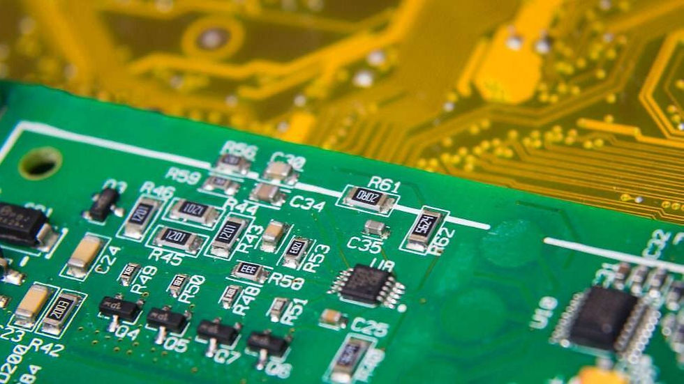
Printed circuit board (PCB) demand appears to be on the rise because, as was already said, it is widely utilized across many industries. The truth is that a PCB designer can do a lot at the macro board level. This is to fit more components onto smaller boards. Due to their adaptability, HDI PCBs have gained popularity in recent years, which is a cutting-edge multilayer PCB design technology. The HDI PCB market is primarily driven by the 10-layer HDI. Electronics can now fit wherever they are needed due to HDI design, which allows designers to produce smaller products and sophisticated boards with better signal integrity in the future.
Boost your product design with HDI PCB Stack-ups! The Falcon-233CRS leverages these advanced PCB designs to deliver compact, powerful solutions.
What is an HDI PCB?
HDI stands for High-Density Interconnect. It refers to the usage of any layer HDIs, including buried, blind, and micro vias, to construct compact boards. The High-Density Interconnect PCB is small, lighter in weight and size, cost-effective, and features high-density elements like fine sequential lamination, lines, and spaces, blind and buried vias, microvias, and via-in-pad techniques that improve the electrical performance of embedded devices while also reducing size and weight. In comparison to traditional PCB boards, the HDI PCB uses thinner materials and fewer layers in its manufacturing, which improves its performance and effectiveness.
If you can account for EMI/EMC factors, decreasing signal paths throughout your board will increase signal integrity and electrical performance.
Benefits of HDI PCB
The following is a quick summary of the benefits of employing this approach,
Using HDI Technology, you may add more components to the board which is ideal while keeping it lightweight, compact, reliable, and performance. This is due to the ability to insert pieces on both sides of high-density boards.
It has a sturdy and durable construction, and it slows thermal degradation, which also helps durability.
It has a low power consumption, making it suited for applications that use batteries, such as smartphones and tablets.
These boards are superior protection against severe environments because of the use of stacked vias.
A 6-layer HDI board can perform the same functions as an 8-layer through-hole board without sacrificing quality.
The specifics, functionality, and dependability of your printed circuit board can all be affected by the HDI Stack type.
Design considerations for HDI PCBs
HDI PCB design is comparable to a complex puzzle. You should take into account the following design principles when creating your HDI PCB:
It is used to prevent impedance from impairing signal integrity.
All the radiation considerations, such as preventing unintended antennas and noise are applied.
HDI frequently results in better thermal performance. But you should also consider the thermal stability of the micro vias and trace widths when designing high-speed signals.
A lot of complexity is added to the design process when physical, electromagnetic, and thermal issues must be taken into account. Multi-dimensional PCB challenges are solved easily because of advancements in EDA software tools. EDA stands for Electronic Design Automation.
Types of HDI PCB Stack-up
During the assembling process, the manufacturers can take one of the three ways. These consist of:
Regular lamination, which uses plated vias or through-holes.
Utilizing Micro vias to build up lamination.
Sequential lamination with bling plated through and hidden vias.
The common types of stack-ups are listed below,
1+N+1 – High-density connectivity layers are present in one build-up on PCBs.
i+N+I (i≥2) – PCBs have two or more layers that are built up with high-density interconnections. Microvias on different subgroups may be stacked or staggered.
i+bN+i (i≥2) – consists of buried vias
Any layer HDI – A PCB has high-density connector layers on every layer. This enables flexible interconnection between conductors on any layer of the PCB using copper filler stacked microvia structures.
Which Stackup Type Is Best for Your PCB?
The dependability and performance of a printed circuit board can be assessed using the chosen Stack-up method. Because of this, this article will offer helpful advice on high-density PCB stackups and how to pick the best one for your application. More people are using HDI technology because of its unique characteristics. The major goal of adopting an HDI board is to maximize performance and reliability while minimizing PCB size.
The standard uses via types to distinguish HDI stackups from one another
In a High-Density Interconnect PCB, vias are microscopic, conductive holes that join different layers and provide easy signal flow. Four different types of vias, including through-hole vias, stacked vias, blind vias, buried vias, staggered vias, skip vias and microvias, are drilled into an HDI PCB based on the functionality of the PCB.
More HDI PCB manufacturers are constructing laminations with microvias and other cutting-edge features for HDI PCBs. As a result of the traces and vias’ significantly reduced sizes, the microvia HDI PCB design has the advantage of attaining a very high route density with fewer layers. The only practical approach to design with multiple large, fine-pitch BGAs with pitch measuring 0.8 mm or below is to effectively use patterns with microvias, which creates greater space for routing and the opportunity for a lower number of layers in microvia HDI PCBs. In addition to being the most affordable option for high-frequency, high-density boards, HDI technology enhances power and signal integrity in high-frequency PCBs when the stackup configuration is appropriate. Different types of vias in PCB design: selecting the best type for HDI PCB design helps choose an appropriate type of vias for the HDI PCB design requirements.
Tips to Design HDI PCBs
There are a few things you need to bear in mind when we talk about constructing a PCB. For instance, the manufacturing procedure for a four-layer HDI board is not all that different from the assembly process for a normal board.
Mechanical drilling is the first step, followed by through and blind holes. If the HDI board has six layers with two stacks, the procedure can be different. The arrangement of the components on the board is another important factor to take into account. Designing a high-density board is challenging. Because you must keep solderability, install ability, and maintainability,
The PIN spacing for common components should be at least 20 mils due to the importance of spacing. Another crucial rule to follow is to keep signals with high strength as far apart from other indicators as you can.
Use HDI PCB design methods when taking into account components that must be installed on a specific size of the board or when the board’s average connections per square inch are quite high. It is not necessary to use HDI if the ratio of the connections between all the components and test points and the board’s surface area is between 120 and 130 pins per square inch.
It could be a good idea to incorporate a clear isolation effect for the bottom and top layer components in the tracking process. By doing so, you can lessen signal crosstalk in the inner layer. If the signal quality is your first goal, you might even think about drilling blind holes through the pad.

Wrapping Up
Printed circuit boards with HDI, have more wiring per unit space than conventional printed circuit boards. There are numerous potentials for product design with an HDI structure. Cost-effective solutions can be developed by collaborating with your designer and board fabricator and taking into account all of the numerous board construction processes and techniques that are accessible. With us, the customer was successful in meeting the demands of two markets with a single product by utilizing HDI principles in this design, which increased their profitability.
We want you to have access to camera designs that fit your product requirements. Our PCB designers can compactly create the board to satisfy all of your project needs without sacrificing performance or quality, giving you access to improved product performance, increased pricing competitiveness, and new product innovation.
Why settle for less when your designs demand precision and reliability? The AR0233 Color 1080P HDR USB Camera offers unmatched performance through HDI PCB Stack-ups.
If you have any queries, feel free to Contact Us.
